I don't know about you guys but I have had my fill of trying to do ink-resist PCB development. It's just too damned difficult to get good results and usually ends up with me trying to draw in tracks and things with a etch resistant pen.
I finally decided to try out the UV exposure method, but after doing some homework on exposure units I quickly realized that they are a serious rip-off. The guys are charging thousands of Rands for what is pretty much a box with some UV tubes in them, so I decided to make my own.
I found a pallet ramp thrown out at work and decided to load it up into my car. Why? Because the thing was made from 18mm birch ply!
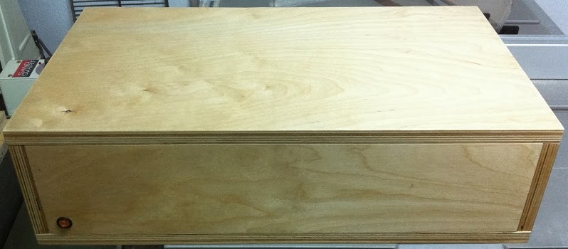
So here is my UV exposure box from the front. It is made from that pallet ramp birch ply. You can see I have a illuminated switch on the bottom left corner.
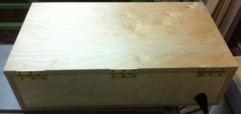
and here is the back. 3 brass hinges, and an IEC connector:
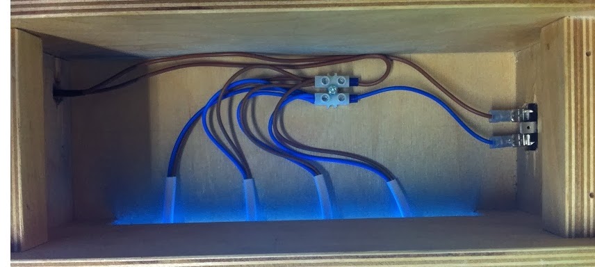
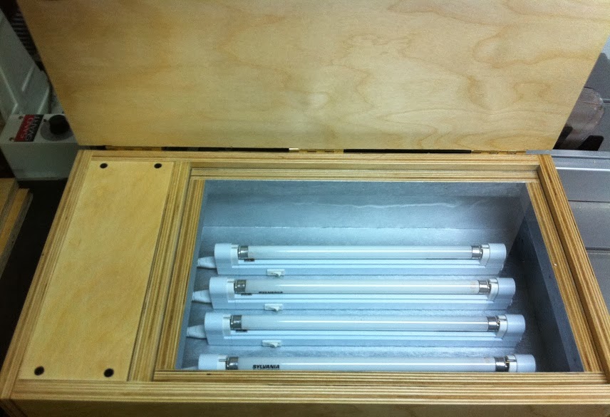
Internal wiring for the 4x UV lamps:
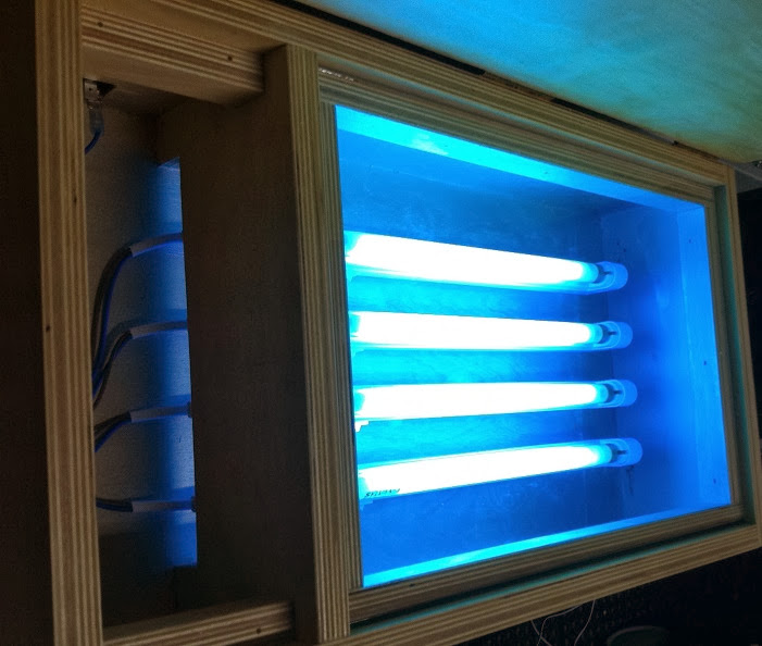
Lights switched on:
Lights switched off. You can see I painted the actual light box with metallic silver paint. This is to create some kind of reflector from the inside. No idea whether it works or not but it is there with beautiful paint runs and all:
Next, you need to figure out how long to expose the PCB, how long to develop it, etc. That is a bit of a mission to put it mildly.
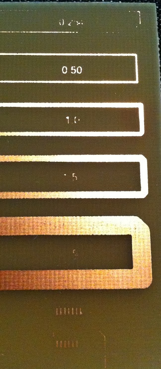
Here you can see what the PCB looks like when its been exposed too long - lots of detail lost and not a great etch in general. The text is the actual track width in mm:
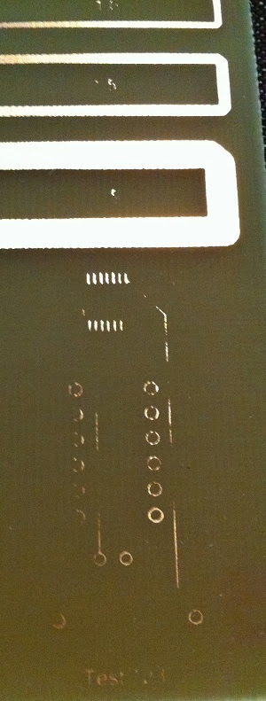
Another part of the board. Pretty bad results:
And here you can see what it looks like when you have a better exposure time. The top part is a TSSOP14, and the bottom is a DIP 12 with some random tracks drawn in:
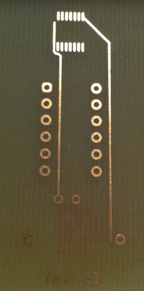
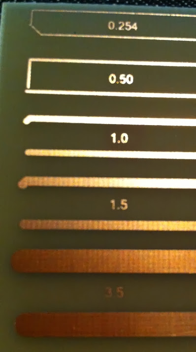
And here is the pic of the tracks. The photo isn't great, but you can see the text and the tracks are pretty good - even down to 0.254mm:
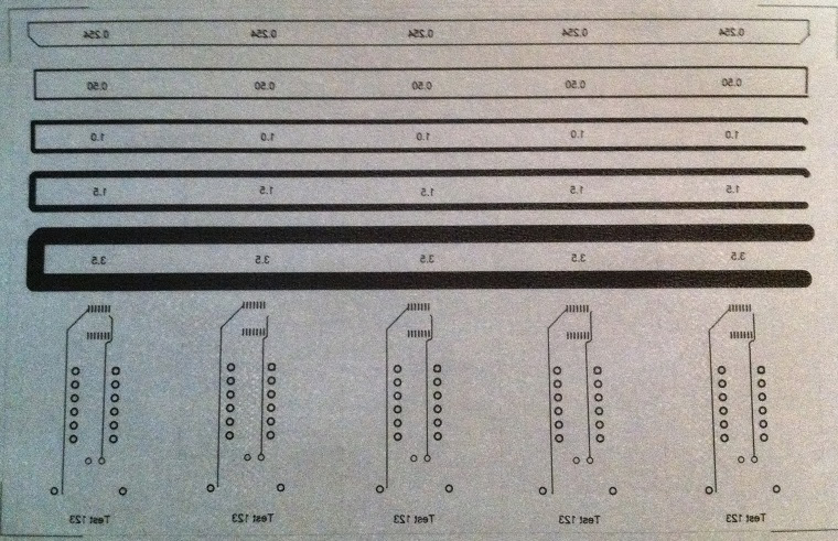
Finally, here is the artwork. I tried laser transparencies, but they didn't give me great results, so I ended up with 60 GSM tracing paper which is pretty thin stuff. Obviously the artwork is mirror image printed because the printed side sits directly on the board:
Great stuff, so now I can start screwing around nicely! Can't wait to get some actual boards out!
Cheers,
Ian.
I finally decided to try out the UV exposure method, but after doing some homework on exposure units I quickly realized that they are a serious rip-off. The guys are charging thousands of Rands for what is pretty much a box with some UV tubes in them, so I decided to make my own.
I found a pallet ramp thrown out at work and decided to load it up into my car. Why? Because the thing was made from 18mm birch ply!
So here is my UV exposure box from the front. It is made from that pallet ramp birch ply. You can see I have a illuminated switch on the bottom left corner.
and here is the back. 3 brass hinges, and an IEC connector:
Internal wiring for the 4x UV lamps:
Lights switched on:
Lights switched off. You can see I painted the actual light box with metallic silver paint. This is to create some kind of reflector from the inside. No idea whether it works or not but it is there with beautiful paint runs and all:
Next, you need to figure out how long to expose the PCB, how long to develop it, etc. That is a bit of a mission to put it mildly.
Here you can see what the PCB looks like when its been exposed too long - lots of detail lost and not a great etch in general. The text is the actual track width in mm:
Another part of the board. Pretty bad results:
And here you can see what it looks like when you have a better exposure time. The top part is a TSSOP14, and the bottom is a DIP 12 with some random tracks drawn in:
And here is the pic of the tracks. The photo isn't great, but you can see the text and the tracks are pretty good - even down to 0.254mm:
Finally, here is the artwork. I tried laser transparencies, but they didn't give me great results, so I ended up with 60 GSM tracing paper which is pretty thin stuff. Obviously the artwork is mirror image printed because the printed side sits directly on the board:
Great stuff, so now I can start screwing around nicely! Can't wait to get some actual boards out!
Cheers,
Ian.