Something easy this time: improving a Gustard USB bridge.
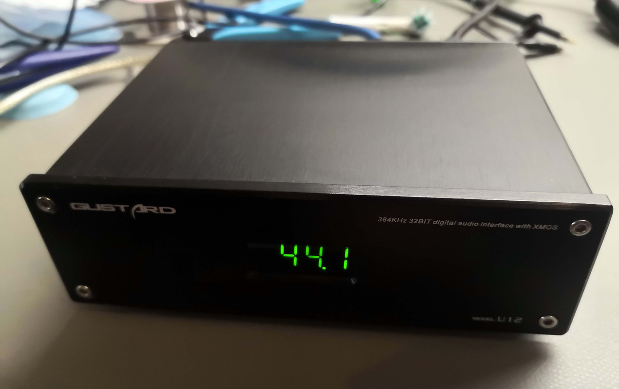
Got it cheap on the forum and it will serve as my lab bridge to easily generate a number of outputs, even I2S and has a useful display.
Despite the technology inside being quite good (XMOS asynchronous bridge with good quality oscillators and power supplies with a Xilinx CPLD), the reviews are fairly mediocre. I also saw on ASR a measurement of it showed some discrepancies with the S/PDIF and AES3 outputs so I thought I'd take a peek myself.
What I found was not just incorrect voltage levels of both outputs, but also impedance mismatch of the S/PDIF. I need correct signals for a testing device, so I set out to make a little board and some other improvements too while I was at it:
- Create a little bord that ties in between the CPLD and the output transformers. Ideally I'd have included the transformers too but there is just no space, so mine had to slot in the middle. The Gustard's CPLD drives the S/PDIF and AES3 outputs using four TTL pins in parallel per output via a 33R resistor each, which gives ample current drive but it's not very robust and not a proper line driver. So the board takes the input signal from the CPLD, translates it to 5V and feeds it to dedicated fast line drivers together with clamping protections diodes. The board is powered with very low-noise local regulators. It's kept in place with a dollop of hot-melt glue.
- Change the overall termination method of both outputs to a much more accurate method than the standard single-resistor method. My termination scheme is much more complex and also includes some specific snubbers to counteract the transformer inductance as well as taking line driver finite output impedance into account.
- Change the 45.158MHz oscillator used for 44.1kHz and its multiples to the super-low jitter Crystek CHD-975 type. I only changed the one since they are very expensive (about R600 each) and there's enough that can be done with this one for precise measurements.
- Double the power supply capacitors from 4400uF to 9400uF
- Change the rectifier diodes from regular PN types to Schottky
- Add snubbers to the rectifiers
- Clean circuit board flux, connectors and chassis
The most notable thing was the improved waveform shape from the S/PDIF's improved termination and line driver. Amplitude is also up from 360mV to 460mV (ideally it should be 500mV but this is perfectly fine). The AES3 output also improved but I don't have a proper terminator at the scope for 110Ohm balanced signals.
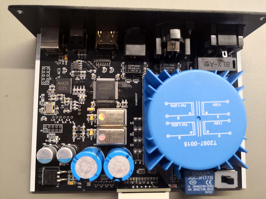
Below is a pic of the inside unit before changes:
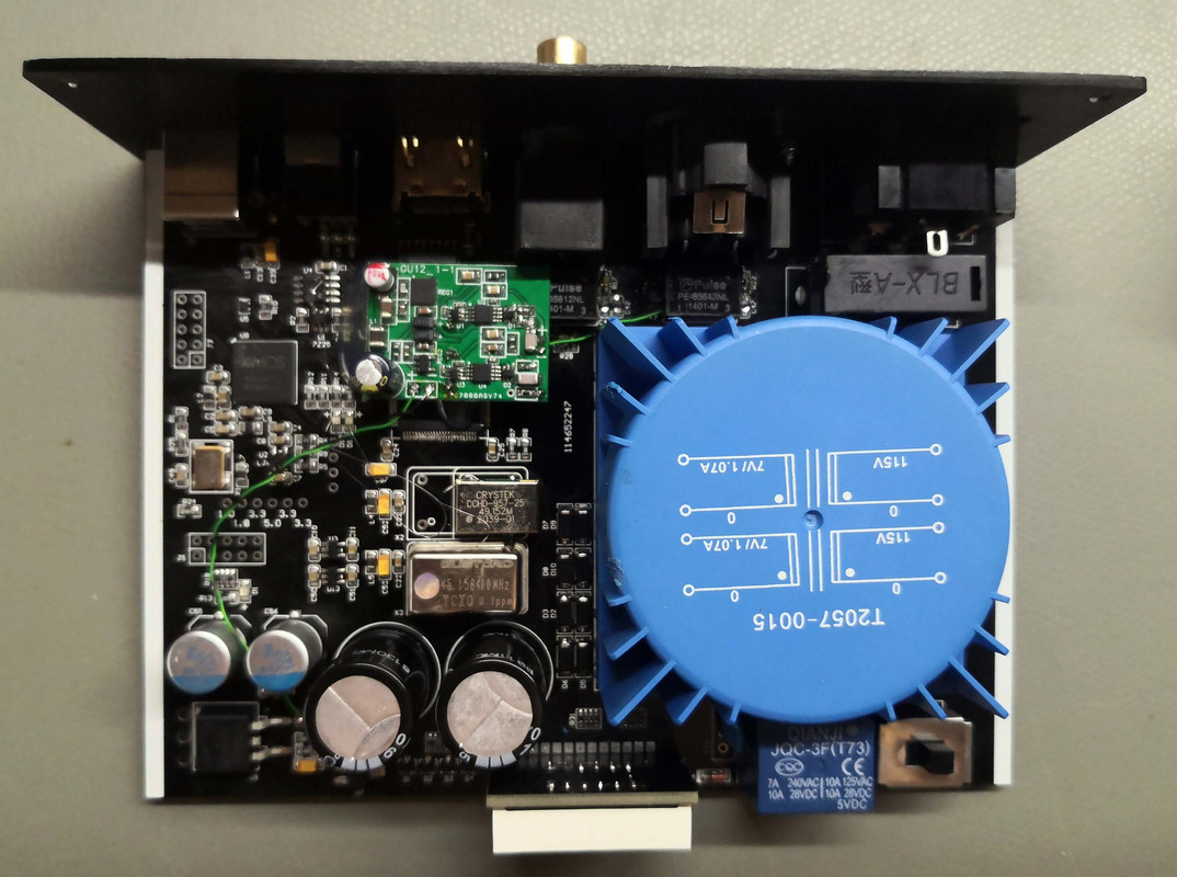
Here is after:
S/PDIF output, stock:
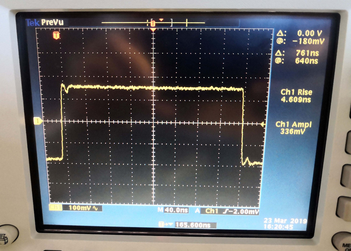
Note the little 'steps' as the edges rise and fall, and the 336mV amplitude
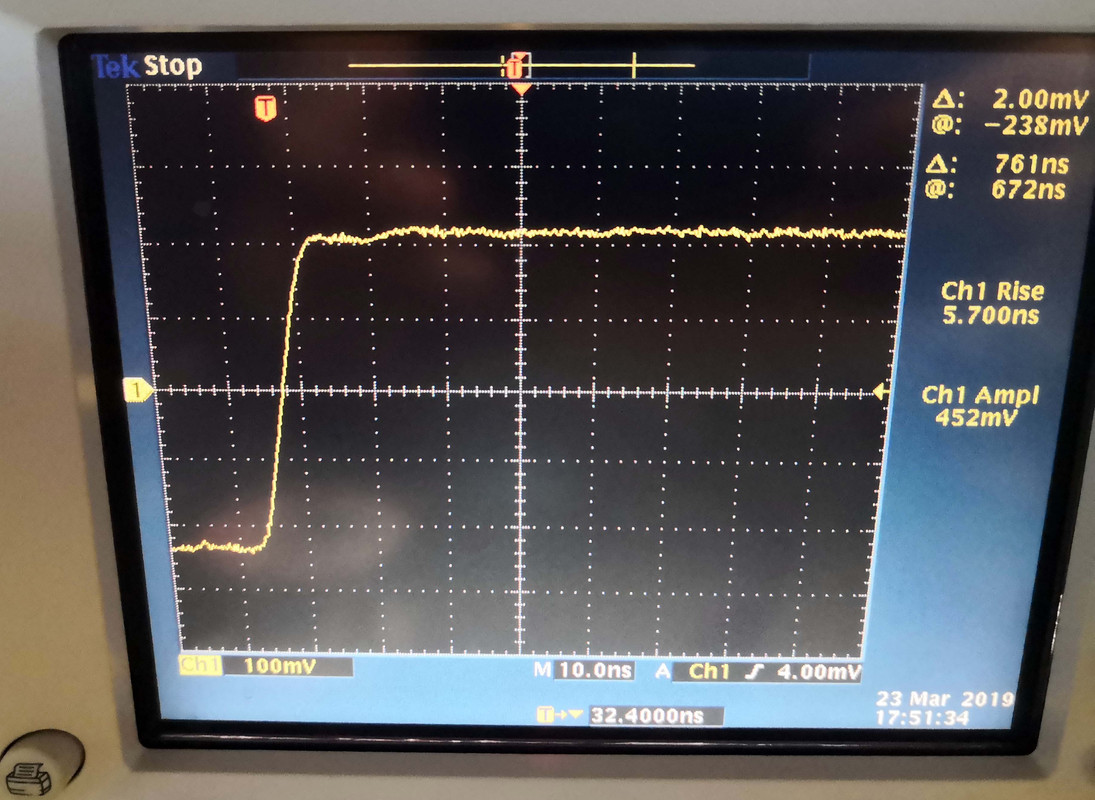
S/PDIF output, new:
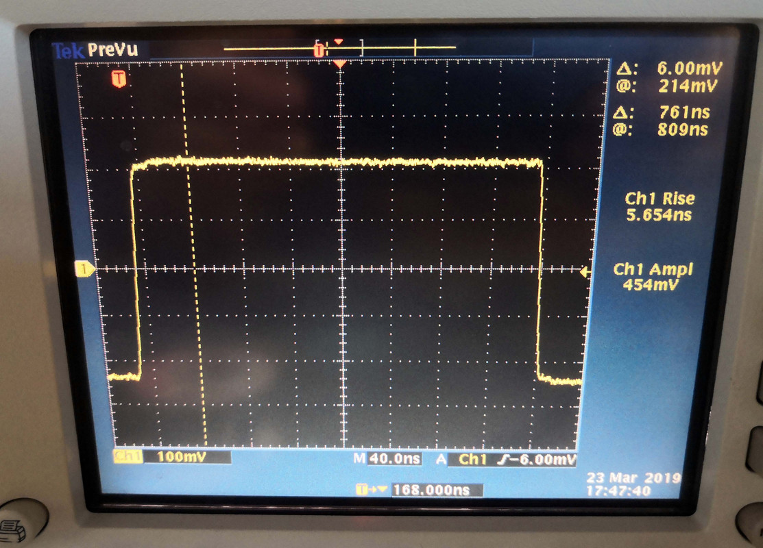
Four things to note:
- Transient response is now almost perfect, with only a tiny step still visible. This is partly due because of mismatch because of RCA cables, but it's pretty much benign.
- Amplitude is now a healthy 454mV
- Noise is lower
- Rise time is a tiny bit higher due to the line driver and protection diodes, but is negligible
Even if stretching the timebase four times, the step is very small:
After everything is closed and done:
Got it cheap on the forum and it will serve as my lab bridge to easily generate a number of outputs, even I2S and has a useful display.
Despite the technology inside being quite good (XMOS asynchronous bridge with good quality oscillators and power supplies with a Xilinx CPLD), the reviews are fairly mediocre. I also saw on ASR a measurement of it showed some discrepancies with the S/PDIF and AES3 outputs so I thought I'd take a peek myself.
What I found was not just incorrect voltage levels of both outputs, but also impedance mismatch of the S/PDIF. I need correct signals for a testing device, so I set out to make a little board and some other improvements too while I was at it:
- Create a little bord that ties in between the CPLD and the output transformers. Ideally I'd have included the transformers too but there is just no space, so mine had to slot in the middle. The Gustard's CPLD drives the S/PDIF and AES3 outputs using four TTL pins in parallel per output via a 33R resistor each, which gives ample current drive but it's not very robust and not a proper line driver. So the board takes the input signal from the CPLD, translates it to 5V and feeds it to dedicated fast line drivers together with clamping protections diodes. The board is powered with very low-noise local regulators. It's kept in place with a dollop of hot-melt glue.
- Change the overall termination method of both outputs to a much more accurate method than the standard single-resistor method. My termination scheme is much more complex and also includes some specific snubbers to counteract the transformer inductance as well as taking line driver finite output impedance into account.
- Change the 45.158MHz oscillator used for 44.1kHz and its multiples to the super-low jitter Crystek CHD-975 type. I only changed the one since they are very expensive (about R600 each) and there's enough that can be done with this one for precise measurements.
- Double the power supply capacitors from 4400uF to 9400uF
- Change the rectifier diodes from regular PN types to Schottky
- Add snubbers to the rectifiers
- Clean circuit board flux, connectors and chassis
The most notable thing was the improved waveform shape from the S/PDIF's improved termination and line driver. Amplitude is also up from 360mV to 460mV (ideally it should be 500mV but this is perfectly fine). The AES3 output also improved but I don't have a proper terminator at the scope for 110Ohm balanced signals.
Below is a pic of the inside unit before changes:
Here is after:
S/PDIF output, stock:
Note the little 'steps' as the edges rise and fall, and the 336mV amplitude
S/PDIF output, new:
Four things to note:
- Transient response is now almost perfect, with only a tiny step still visible. This is partly due because of mismatch because of RCA cables, but it's pretty much benign.
- Amplitude is now a healthy 454mV
- Noise is lower
- Rise time is a tiny bit higher due to the line driver and protection diodes, but is negligible
Even if stretching the timebase four times, the step is very small:
After everything is closed and done: